


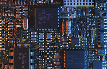
What is a PCB and How It's Made
Feb 10, 2022 22:48
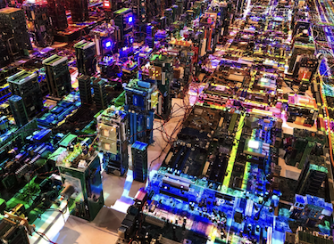
PCBs are a vital part of nearly every electronic device. They are used to connect and support the different parts of a device, and they need to be both reliable and durable. PCBs are made by combining several different materials into a single board. This process begins with the selection of the right substrate material, creating a pattern for the conductors and other components that will be on the PCB, which is then transferred to a copper-clad laminate and serves as the foundation for the PCB. The final step is to add the finishing touches, such as silk screening and plating. Let's explore more closely what it is and how exactly it's made.
So, What Is A PCB?
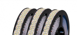
PCBs are usually made out of a polymer-based laminate with layers of alternating electrical conductors and insulating materials. The overall thickness of the board is called the substrate, which can range from less than 1mm to 6 millimeters or more in most cases. The acronym PCB stands for Printed Circuit Boards. However, the term "board" is a bit misleading, since printed circuit boards can take on many different shapes and forms. PCBs were first developed during the Second World War to reduce the number of wiring errors in various military equipment. Since then they have found their way into civilian applications as well, including electrical devices that are used in nearly every home around the world today. There are two types of PCBs - rigid type (used where space is limited) and flexible type (made with thinner copper laminate).
Rigid PCBs
Since rigid PCBs are made using a thicker substrate material they are more durable than flexible circuits. Rigid PCBs can be divided into two types - multi-layer and rigid-flex. Multi-layer boards are made out of multiple layers of substrate, whereas the rigid-flex type is constructed using a flexible base laminate sandwiched between two thicker material sheets.
Flexible PCBs
Flexible PCBs are typically designed to be more lightweight than their multi-layer counterparts. This means they bend more easily and can even be curved to some extent. They are mainly used in applications that require a moderate level of circuit protection, such as smartphone casings or cases for different types of consumer electronics. In the past, flexible circuits were limited by their performance - they couldn't handle high frequencies and higher currents very well, and they were more sensitive to temperature and atmospheric conditions. However, new technologies and materials have made it possible to produce flexible circuits that are just as good as rigid ones.
What is a PCB Used For?
PCBs can be used in any application where electrical circuits need to be controlled electronically. These boards play an essential role in controlling all of the devices we use every day, from ovens and toasters to televisions and computers. They can also be found in all types of vehicles, including planes, trains, and automobiles. When you watch your favorite movie or television show on a DVD or Blu-ray Disc player, PCBs play a vital role in controlling the disc drive and decoding the signal that is transferred to your TV screen. Any type of device that uses electricity either has one or more PCBs inside, helping it perform its intended task.
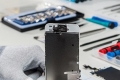
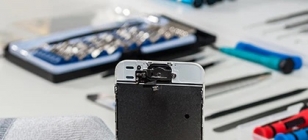
How Are PCBs Made?
There are various steps involved in creating PCB prototypes for consumer products. These include material preparation (substrate choice), board fabrication (creating the circuits), and substrate finishing (the actual manufacture). Let's take a closer look at each of these steps.
Material Preparation
The material used in PCBs is called the substrate, and it can be made out of any number of substances, including epoxy resin, glass fiber, or metal. Once the substrate has been chosen it needs to be sliced into thin sheets that are several inches wide. The most common thickness for rigid substrates is 1/16" (1.5mm), but flexible circuits tend to use thinner laminates that are between 0.001" (0.025mm) and 0.010" (0.25mm). Since various types of conductors can be used on PCBs (copper, nickel, gold, etc.), the individual slices are plated to ensure that all of the proper components are in place.
Board Fabrication
Once the substrate has been prepared it is ready to be engraved with various circuit patterns. The etching process uses photolithography (a complex photo development system) to produce images on each side of the PCB. This includes placing copper foil patterns on one or both sides, depending on whether single-sided or double-sided boards are being used. Once the photoresist layer (coating) is applied and hardened, light passes through a transparent mask (or reticle), exposing only certain parts of the coating. Using this method, it's possible to create either single-sided or double-sided boards by completely covering one side with a conductive material using one mask, removing the exposed coat with chemical etching (a type of liquid acid), and then using a second mask to cover the opposite side with conductive material. The first step in this process is to place an electronic design on the board. This process uses data that has been programmed into software by engineers or technicians, depending on who is creating the PCBs.
Printing Solder Masks
The next step in manufacturing is to print solder masks onto flexible substrates. These are typically used for rigid boards as well since they protect exposed conductors against corrosion and provide insulation between circuit layers. Finally, another layer of lacquer may be placed over the board once all of these processes have been completed to ensure that it can withstand extreme temperature changes during use.
Board Finishing
At this point, the board is ready to be used, but it may also be treated with several different types of coatings or enamel. These include drilled holes for mounting components (such as switches, displays, and other peripherals), solder masks, power plane layers (free of charge-plating), silk screen printing (for identification purposes), PCB edge finish coating (to protect against corrosion or wear), and finishing lacquer for protection.
The process of creating PCB prototypes for consumer products is no simple task but can be completed by engineers and technicians with proper training and experience in this particular field. It is important to understand the different components used in PCBs and how they work together to form a complete circuit. By taking a closer look at these various steps, you will gain a better understanding of what is involved in producing printed circuit boards for consumer products.