


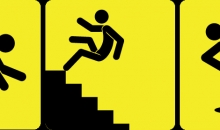


4 Common failures you must know when designing PCB
Jun 19, 2017 07:51
Today’s electronics, starting from smartphones to complex computers, is incomplete without Printed Circuit Boards (PCB). These boards are self-contained modules of various interconnected components via a complex array of circuits.
To protect this array of connections, PCBs have many layers of copper traces and plastic.
Designing and manufacturing process of PCBs are quite complicated and thus it is highly probable that many PCB failure issues come up. We are here to state 4 common failures when manufacturing a PCB – the ‘What’, ‘Why’ & ‘How’.
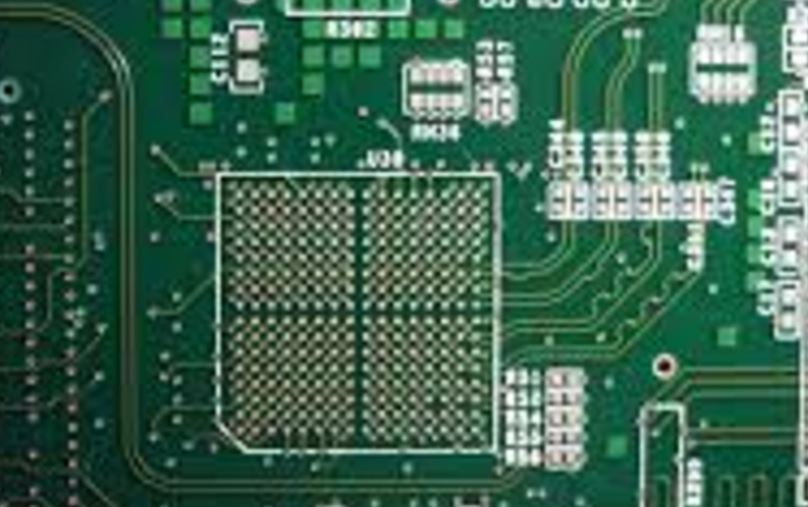
In a PCB, Plated-thru copper holes allow the flow of electricity from one side to the other. For the drilling these holes, the material is punctured throughout the way using PCB fabricator. After the creation of these holes, the surface of the material is layered with copper chemically through the process of electroplating. Electroplating deposits a thin layer of electro less copper about 1 micron thick over the walls of the holes and this process is known as Deposition.
The Deposition process may create voids in the plating sometimes. Plating voids are gaps or holes in the plating of the PCB due to problems during the deposition process. These voids are not favorable since they do not allow the current flow through that particular hole and thus results in defective PCB.
Why are Plating Voids formed?
The reason behind the formation of plating voids along the walls of holes is due to contamination of the material, air bubbles, insufficient cleaning and catalyzation of copper during drilling of plated-thru copper holes.
How to avoid the formation of Plating Voids?
Plating voids formed due to contamination and air bubbles can be avoided by a cleansing process in the material after drilling holes.
Faulty drilling can be avoided by having the required number of drill hits, drill in-feeds and drill speeds according to the manual provided by the manufacturer.
Electromagnetic Compatibility (EMC) is the generation, propagation and reception of electromagnetic (EM) energy.
Electromagnetic interference (EMI) is the unwanted effects of EMC that causes damage to the PCB.
Why do these Electromagnetic issues come up?
The electromagnetic issues – EMC & EMI basically come up due to one of the wide variety of probable flaws in design. PCB designs can be improved using professional connectors manufactured by the leading PCB Connectors Manufacturer – Scondar.
How to reduce EMI?
Electromagnetic Interference (EMI) can be brought down by increasing the PCB’s area and making compartments in the PCB for EMI. Moreover, orthogonal angles must be avoided for almost all the components in the PCB as they increase EMI.
Whenever the PCB manufacturer expert doubts EMI to occur during the prototyping, he can use shielded cables and metal package to avoid EMC and thus lower down the possible EMI.
On a Printed Circuit Board, the layer on the top of the copper layer is known as the Solder Mask and is meant to insulate copper from contact with other metal or solder. Moreover, solder mask also prevents corrosion and prevents electrocution of PCB handlers.
Why is the absence of solder mask between pads a problem?
During assembly, the absence of solder mask between pads causes unnecessary exposure of copper and thus results in the formation of solder bridges between pins shorting the circuit and reduces the protection from corrosion.
This defect is formed due to an oversight during the designing of the circuit board.
How to prevent this defect?
This defect can be avoided by checking the design of the PCB before sending to the manufacturer and by making sure that the manufacturer has a proper DFM protocol.
Acid Traps are formed due to the accumulation of acid in the acute angles of the PCB during the etching process. Due to this, the acid is trapped for a longer duration than required and thus result in a defective circuit since the acid destroys the connection.
Why are Acute Angles formed?
Acute angles can be formed due to simple human error. There are also chances that the design software programs cause acute angles in the circuits.
How to prevent the formation of Acute Angles?
Acute angles can be prevented by avoiding human error – double-checking the design. These can also be tackled using DFM check.
Whenever you are designing a PCB, these 4 failures must be kept in mind. Most of the faults in PCB manufacturing are due to the flaws in quality of the PCB. You can improve the quality of your PCB by using latest high-density, high-speed PCB interconnects like board to board connector to offer a reliable solution at a reasonable price.
To protect this array of connections, PCBs have many layers of copper traces and plastic.
Designing and manufacturing process of PCBs are quite complicated and thus it is highly probable that many PCB failure issues come up. We are here to state 4 common failures when manufacturing a PCB – the ‘What’, ‘Why’ & ‘How’.
1. Plating Voids formed during Deposition Process
What are Plating Voids?In a PCB, Plated-thru copper holes allow the flow of electricity from one side to the other. For the drilling these holes, the material is punctured throughout the way using PCB fabricator. After the creation of these holes, the surface of the material is layered with copper chemically through the process of electroplating. Electroplating deposits a thin layer of electro less copper about 1 micron thick over the walls of the holes and this process is known as Deposition.
The Deposition process may create voids in the plating sometimes. Plating voids are gaps or holes in the plating of the PCB due to problems during the deposition process. These voids are not favorable since they do not allow the current flow through that particular hole and thus results in defective PCB.
Why are Plating Voids formed?
The reason behind the formation of plating voids along the walls of holes is due to contamination of the material, air bubbles, insufficient cleaning and catalyzation of copper during drilling of plated-thru copper holes.
How to avoid the formation of Plating Voids?
Plating voids formed due to contamination and air bubbles can be avoided by a cleansing process in the material after drilling holes.
Faulty drilling can be avoided by having the required number of drill hits, drill in-feeds and drill speeds according to the manual provided by the manufacturer.
2. Electromagnetic Compatibility and Interference in circuit board design
What are EMC and EMI?Electromagnetic Compatibility (EMC) is the generation, propagation and reception of electromagnetic (EM) energy.
Electromagnetic interference (EMI) is the unwanted effects of EMC that causes damage to the PCB.
Why do these Electromagnetic issues come up?
The electromagnetic issues – EMC & EMI basically come up due to one of the wide variety of probable flaws in design. PCB designs can be improved using professional connectors manufactured by the leading PCB Connectors Manufacturer – Scondar.
How to reduce EMI?
Electromagnetic Interference (EMI) can be brought down by increasing the PCB’s area and making compartments in the PCB for EMI. Moreover, orthogonal angles must be avoided for almost all the components in the PCB as they increase EMI.
Whenever the PCB manufacturer expert doubts EMI to occur during the prototyping, he can use shielded cables and metal package to avoid EMC and thus lower down the possible EMI.
3. Absence of Solder Mask between Pads
What is a Solder Mask?On a Printed Circuit Board, the layer on the top of the copper layer is known as the Solder Mask and is meant to insulate copper from contact with other metal or solder. Moreover, solder mask also prevents corrosion and prevents electrocution of PCB handlers.
Why is the absence of solder mask between pads a problem?
During assembly, the absence of solder mask between pads causes unnecessary exposure of copper and thus results in the formation of solder bridges between pins shorting the circuit and reduces the protection from corrosion.
This defect is formed due to an oversight during the designing of the circuit board.
How to prevent this defect?
This defect can be avoided by checking the design of the PCB before sending to the manufacturer and by making sure that the manufacturer has a proper DFM protocol.
4. Acid Traps formed during the etching process
What are Acid Traps?Acid Traps are formed due to the accumulation of acid in the acute angles of the PCB during the etching process. Due to this, the acid is trapped for a longer duration than required and thus result in a defective circuit since the acid destroys the connection.
Why are Acute Angles formed?
Acute angles can be formed due to simple human error. There are also chances that the design software programs cause acute angles in the circuits.
How to prevent the formation of Acute Angles?
Acute angles can be prevented by avoiding human error – double-checking the design. These can also be tackled using DFM check.
Whenever you are designing a PCB, these 4 failures must be kept in mind. Most of the faults in PCB manufacturing are due to the flaws in quality of the PCB. You can improve the quality of your PCB by using latest high-density, high-speed PCB interconnects like board to board connector to offer a reliable solution at a reasonable price.